Description
LXF33K00 5.4GSPS, 12 bit Low latency wideband transceiver
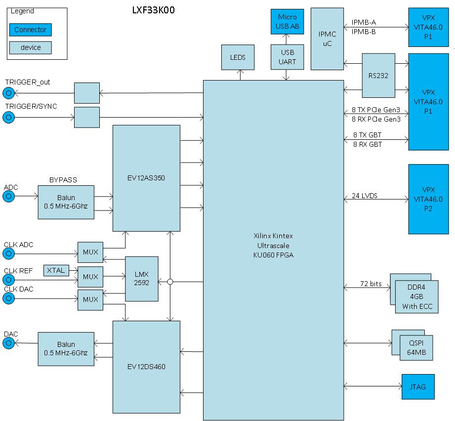
A combination of low latency wideband analogue to digital converter, digital to analogue converter and Xilinx Kintex Ultrascale makes the LXF33K00 the ideal platform for embedded signal processing applications such as Electronic Warfare, Wideband Radar transceiver or wideband communication applications. The LXF33K00 is fully compliant to the Vita65.0 openVPX standard and the VITA46.11 VPX shelf management standard.
Analog input and output
With an analogue input stage that has a very wide input bandwidth from 0.5MHz up to 4.8GHz and the low latency 5.4Gsps ADC from E2V(EV12AS350A) the LXF33K00 delivers unmatched performance with regards to SFDR, close in phase noise and latency (7.2 ns). Sampling at 5.4 Gsps offers an instantaneous bandwidth of 2.7GHz. Surpassing the analogue input, the analogue output offers an even lower latency (1.2 ns) using the EV12DS460 DAC device from E2V. The output bandwidth ranges from 0.5MHz to 6GHz, and the instantaneous output bandwidth is 1.35GHz. Both the ADC and DAC offer 12-bits resolution further contributing to achieving best in class signal to noise ratios.
Clock tree
The onboard low-noise clock generator ensures easy integration into small single board systems as well as standalone operation. For larger systems it is possible to easily synchronize multiple boards by providing an external reference clock. This is a special feature offered by the onboard clock PLL.
FPGA and Memory
The LXF30K00 comprises a Xilinx Kintex Ultrascale KU060 user programmable FPGA. Most of the logic, block RAM and all DSP resources are available for customer processing. With the KU060 FPGA the LXF33K00 offers; 663 K logics cells, 1,080 36 Kbit RAM blocs, 3 PCIe interface blocks and 2,760 DSP48 slices. The FPGA speed grade is -2. The LXF3000 FPGA connects to one 72 bits wide DDR4 memory bank, offering a total of 4GB of storage with error correction codes. At 2400 Mhz the memory bank offers a total bandwidth of 21.6 GB/s. For FPGA configuration, the LXF33K00 has a 64MB QSPI FLASH memory.
VPX interface
At the P1 connector, the LXF33K00 has two fat pipes that form the data plane. At the expansion plane on P1 there are also two FAT pipes. Each fat pipe can be divided into two thin pipes or four ultra thin pipes. A total of thirty-two user definable LVDS signals connect between the FPGA and the VPX P2 connector. The LXF33K00 supports two types of cooling. The board can be ordered in the conduction-cooled version for harsher environmental conditions. Otherwise, the board is available in an air-cooled version.
Applicatons
- Systems that will benefit greatly from this product are:
- Advanced digital radio frequency memory (DRFM)
- Radar waveform generators and receivers
- Telecommunication systems
- Experimental Physics
- Analog record and playback systems
- Aerospace and test instrumentation
- Software-defined radio (SDR)