Description
LXF31K14 – four channel 3U VPX, 310Msps ADC/DAC with 16-bit resolution
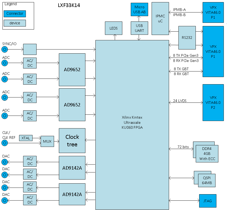
Four 16-bit A/D channels with up to 310 Msps data rate and four 16-bit D/A channels with up to 310 Msps data rate and a 1.24 Gsps update rate combined with a Xilinx Kintex Ultrascale makes the LXF33K14 the ideal platform for embedded signal processing applications such as Electronic Warfare, Wideband Radar transceiver or MIMO communication applications. The LXF33K14 is fully compliant to the Vita65.0 openVPX standard and the VITA46.11 VPX shelf management standard.
Analog input and output
Depending on the application requirements, it is possible to order the LXF33K14 with either a DC coupled or an AC coupled analogue front end. The DC coupled interface is meant for signal acquisitions and playback in the first Nyquist zone while the AC coupled inputs also offers the option for signal acquisition and playback in the second Nyquist zone. Both the ADC and DAC offer 16-bits resolution further contributing to achieve best in class signal to noise ratios.
Clock tree
The onboard low noise clock generator ensures easy integration into small single board systems as well as standalone operation. For larger systems it is possible to easily synchronize multiple boards by providing an external reference clock. This is a special feature offered by the onboard clock pll.
FPGA and Memory
The LXF31K18 comprises a Xilinx Kintex Ultrascale KU060 user programmable FPGA. Most of the logic, block RAM and all DSP resources are available for customer processing. With the KU060 FPGA the LXF31K18 offers; 663 K logics cells, 1,080 36 Kbit RAM blocs, 3 PCIe interface blocks and 2,760 DSP48 slices. The FPGA speed grade is -2. The LXF31K18 FPGA connects to one 72 bits wide DDR4 memory bank, offering a total of 4GB of storage with error correction codes. At 2400 Mhz the memory bank offers a total bandwidth of 21.6 GB/s. For FPGA configuration the LXF31K18 has a 64MB QSPI FLASH memory.
VPX interface
At the P1 connector the LXF31K18 has two fat pipes that form the data plane. At the expansion plane on P1 there are also two FAT pipes. Each fat pipe can be divided into two thin pipes or four ultra thin pipes. A total of thirty-two user definable LVDS signals connect between the FPGA and the VPX P2 connector. Two types of cooling are supported by the LXF31K18. For the harsher environmental conditions, the board can be ordered in the conduction cooled version. Otherwise the board is available in an air-cooled version.
Applications
Systems that will benefit greatly from this product are:
- Digital Beam Forming
- MIMO Applications
- Radar waveform generators and receivers
- Telecommunication systems
- Experimental Physics
- Analog record and playback systems
- Aerospace and test instrumentation
- Software-defined radio (SDR)