Select Page

TEI0009-02-055-8CA

£150.00


Cyclone 10 LP RefKit 10CL055 Development Board, 32 MByte SDRAM, 16 MByte Flash


14 in stock

Description

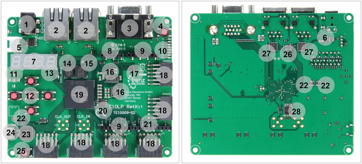
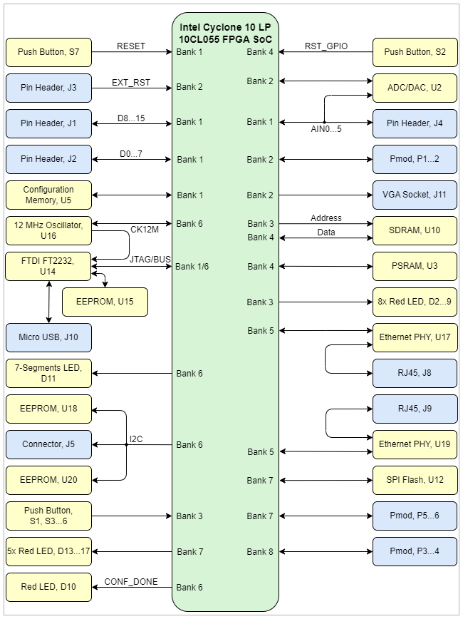
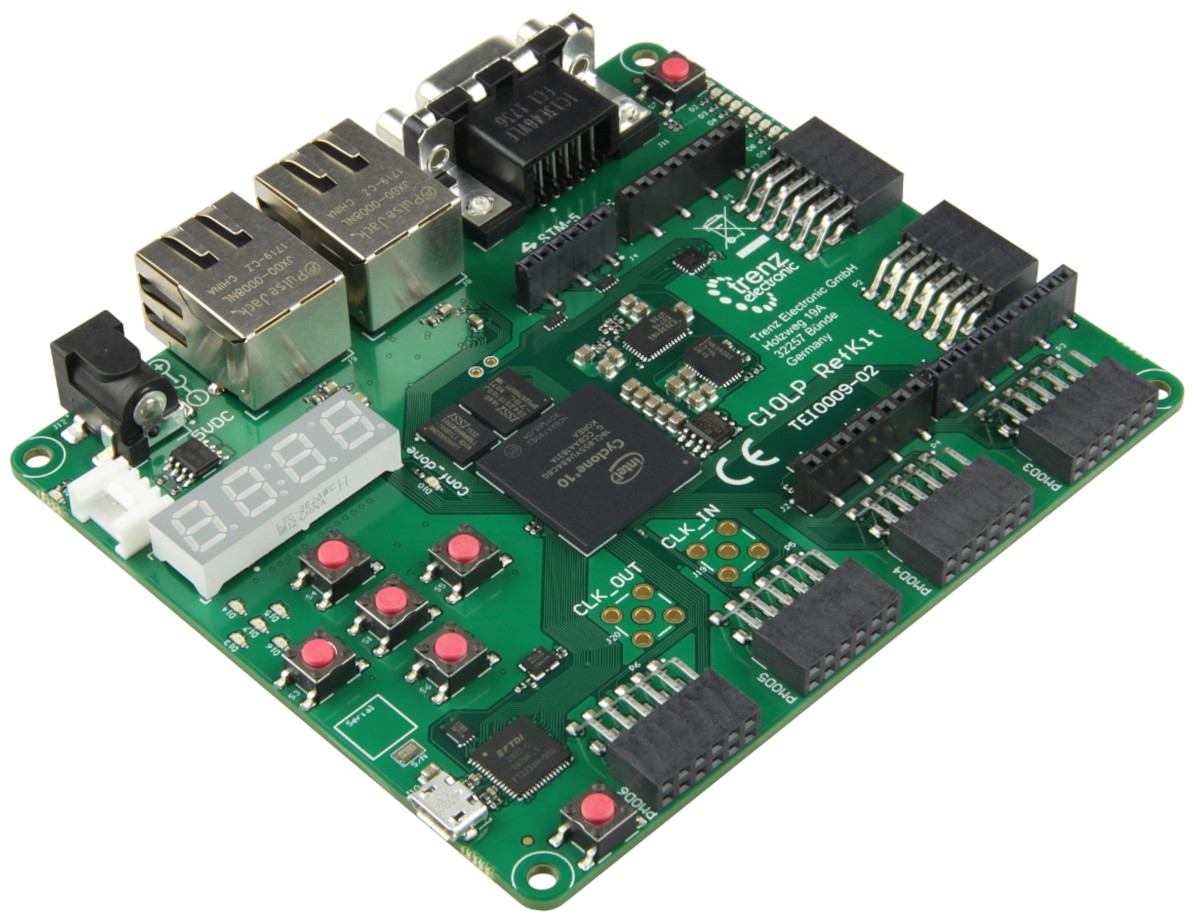
The Cyclone 10 LP Reference Kit is the worldwide first development board with a 55kLE Intel Cyclone 10 LP and a huge variety of interfaces for many applications. The board is fully qualified and ready to use for end products and can also be ordered in customized variants exactly according your requirements.

This reference design is bundled with a FREE evaluation edition of the low-cost, commercially proven, high performance memory controller IP supplied by Synaptic Laboratories Ltd (SLL). This free IP evaluation license never expires, and no customer registration or NIC ID is required.

Click here to find the latest free trials of SLL’s memory controller IP for HyperBus, OctaBus, Xccela Bus, JEDEC xSPI Profile 1.0 and JEDEC xSPI Profile 2.0 for Intel, Microchip, and AMD/Xilinx FPGA. SLL IP is also qualified for use with Trenz Electronic HS CRUVI enabled boards.

Features

  • Intel Cyclone 10 LP FPGA 10CL055YU484C8G, 55 kLE in 484-pin
  • 16 MBit Flash memory (optional up to 32 MBit possible)
  • Integrated USB Programmer 2
  • Connectors
    • Arduino compatible pin headers
    • 6 x Pmod compatible pin headers
    • 1 x Grove connector
    • 1 x D-SUB connector for VGA
    • 2 x SMA connectors (not populated)
  • 256 MBit (optional up to 512 MBit possible) SDRAM
  • 128 MBit (optional up to 512 MBit possible) User Quad-SPI Flash memory
  • 64 MBit HyperRAM (optional up to 128 MBit possible)
  • 2 x MAC-Address EEPROM
  • 2 x Fast Ethernet PHY (10/100 MBit/s)
  • 8-Channel, 12-Bit, Configurable ADC/DAC with On-Chip Reference
  • Status LEDs, Power LED
    • 13 x User LEDs
    • 1 x 7-Segment Display
    • 2 x Reset Buttons
    • 5 x User Buttons

Labelled Image

  1. Power Jack, J12
  2. RJ45 Socket, J8…9
  3. D-Sub Connector, J11
  4. Push Button (Reset), S7
  5. Grove Connector, J5
  6. Undervoltage/Overvoltage Protector, U9
  7. 7-Segment LED, D11
  8. 1×6 Pin Header, J4
  9. 1×8 Pin Header, J2…3
  10. 8x User LEDs (Red), D2…9
  11. 5x User LEDs (Red), D13…17
  12. 5x User Push Buttons, S1 – S3…6
  13. Red LED (CONF_DONE), D10
  14. PSRAM Memory, U3
  15. SDRAM Memory, U10
  16. Voltage Regulator, U4 – U7
  17. AD/DA Converter, U2
  18. 6x Pmod Host Socket, P1…6
  19. Intel Cyclone 10 LP, U1
  20. Serial Configuration Memory, U5
  21. 1×10 Pin Header, J1
  22. EEPROM, U15 – U18 – U20
  23. FTDI USB 2 to JTAG/UART Converter, U14
  24. Micro USB 2.0, J10
  25. Push Button (RST_GPIO), S2
  26. Oscillator, U22
  27. Ethernet PHY, U17 – U19
  28. QSPI Flash Memory, U12

Block Diagram