Description
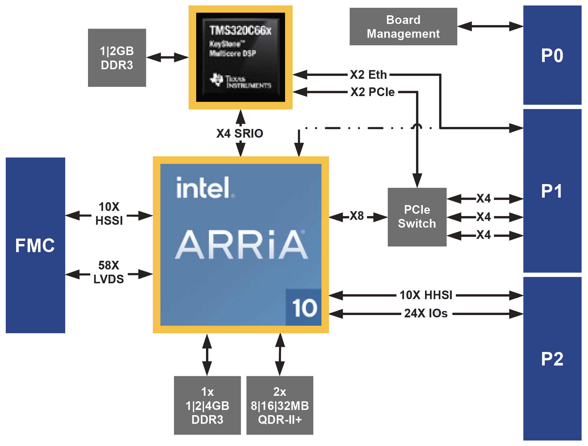
The VF365 is a 3U OpenVPX module that leverages on Intel Arria® 10 SoC FPGA and Texas Instruments KeyStone Multicore DSP technology to provide an ultra-high bandwidth processing platform, ideally suited for computation and bandwidth-intensive applications such as Radar, SIGINT, EW, SDR, Networking and Video.
The Arria® 10 SoC high-performance FPGA fabric provides abundant logic, internal memory and floating-point DSP resources for demanding applications in the industrial, aerospace and other markets.
The hard processor system (HPS) with dual-core ARM Cortex-A9 MPCore processor, on-chip cache, system peripherals and hard memory interfaces provides additional software processing, tightly coupled with the FPGA through high-performance AXI bus bridges.
Processing FPGA
- Arria® 10 SoC family SX Device variants – 570 / 660
- HPS: Dual-core ARM Cortex-A9 MPCore processor @ 1.2 GHz
- Embedded device memory – 36 / 43 Mb
- Embedded device multipliers (18×18) – 3,036 / 3,374
- DDR3 and QDRII+ external memory
- Up to 4GB DDR3 @ 1600MT/s (64-bit bank)
- Up to 64MB QDRII+ SRAM @ 450MHz (two 36-bit banks)
Digital Signal Processor
- Ti KeyStone Multicore C667x family of processors
- Up to 8 cores @ 1.25 GHz
- External memory: Up to 2 GB DDR3 @ 1333 MT/S
FPGA Mezzanine Card (FMC)
- 10x High-Speed Serial Interface lanes (≥ 10Gbps)
- LVDS interface on LA and HA (58 pairs TBC)
VPX Interface
- Comply with OpenVPX MOD3-PAY-3F2U-16.2.12-2 profile
- PCIe Gen2 Data plane (3x Fat Pipes)
- GigE 1000BASE-BX Control plane (2x Ultra-Thin Pipes)
- Payload module with System Controller capability
- Supports FPGA configurable User I/O on P2
- 24x single-ended 2.5V or 3.3V LVCMOS I/Os
- 10x High-Speed Serial Interface lanes (≥ 10Gbps)
Software & Firmware Support
- Board support package with reference application
- Linux PCIe drivers
- FPGA Firmware reference design