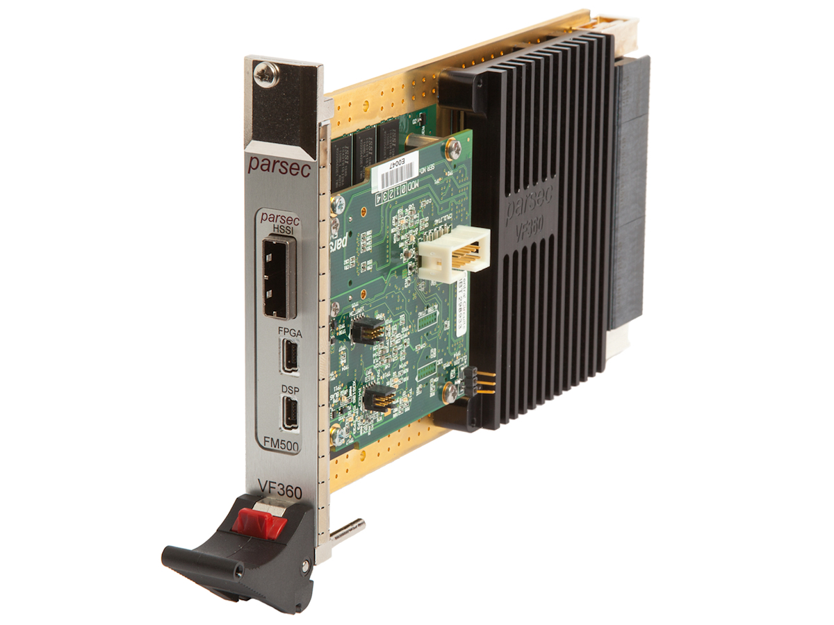
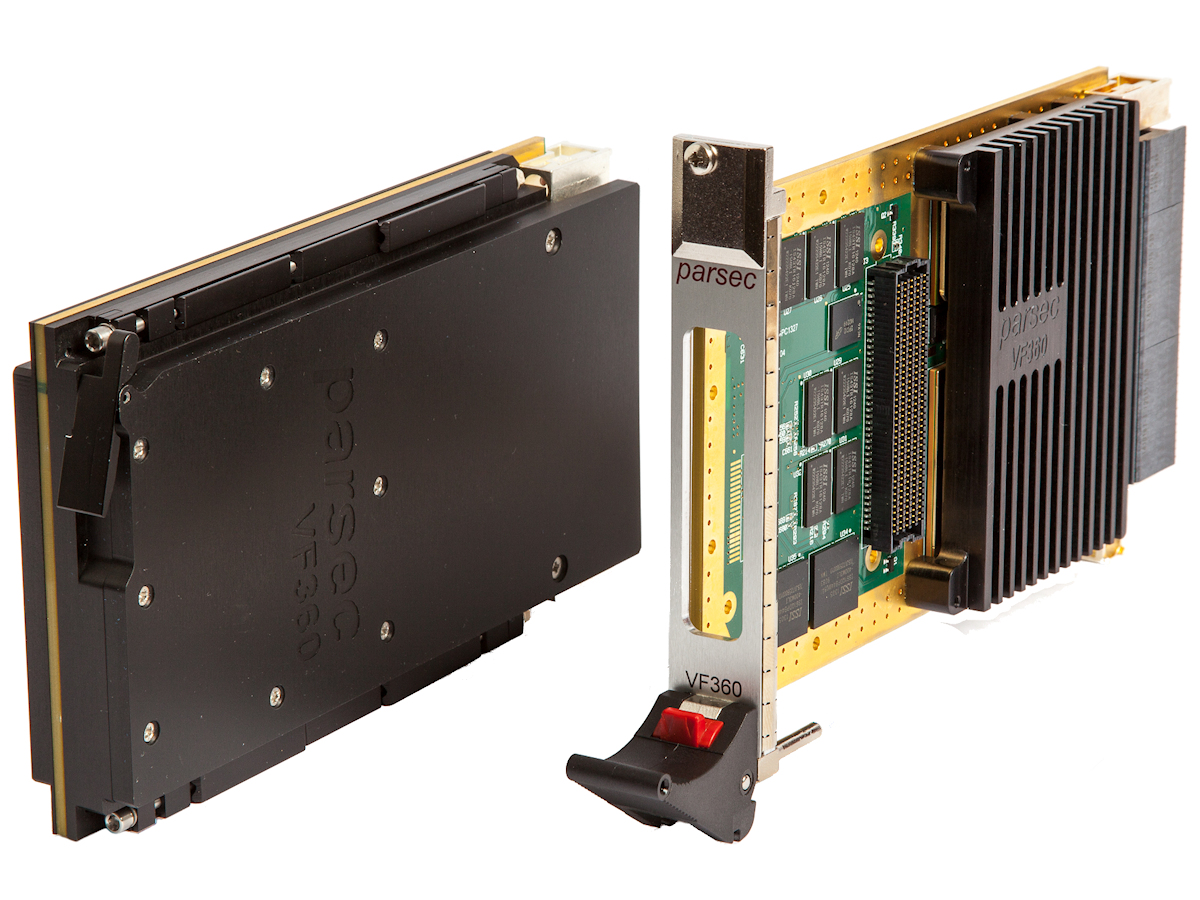
Description
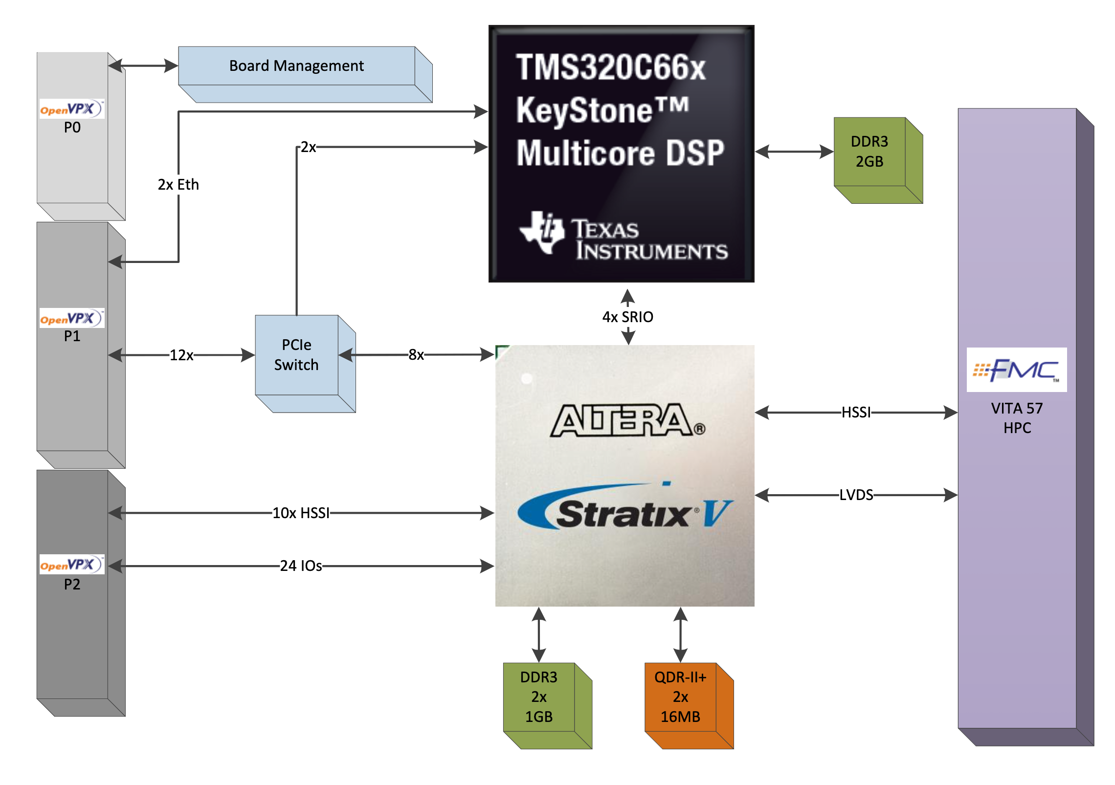
The VF360 is a 3U OpenVPX module that leverages on Intel Stratix® V FPGA and Texas Instruments KeyStone Multicore DSP technology to provide an ultra-high bandwidth processing platform, ideally suited for computation and bandwidth intensive applications such as Radar, Networking, SIGINT, EW, SDR and Video. The onboard multicore DSP from Texas Instruments provides the flexibility to perform complex post processing functions more suited for the processor domain. High bandwidth communication between the DSP and FPGA is provided through both PCIe and Serial Rapid IO (SRIO) interfaces. The Stratix® V FPGA has two banks of dedicated DDR3 and QDRII+ memories for algorithms with high bandwidth and/or large memory size requirements. Highspeed serial interfaces to the OpenVPX data plane and the FMC site creates abundant FPGA IO throughput. The VF360 acts as an FMC carrier to provide a modular solution that accommodates a wide range of I/O requirements. The VF360 conforms to the OpenVPX standard and operates as a Payload module with System Controller capability. Both air-cooled and conduction cooled versions are available. Further flexibility is provided through build options to cater for 10 different FPGAs from Altera’s Stratix® V GX and GS device families.
Processing FPGA:
- Stratix V family in the KF40 (1517 FBGA) package
- GX Device variants: 5SGXA3, 5SGXA4, 5SGXA5, 5SGXA7, 5SGXA9 and 5SGXAB
- GS Device variants: 5SGSD4, 5SGSD5, 5SGSD6 and 5SGSD8
- Embedded device memory: 19-52 Mb
- Embedded device multipliers (18×18): 512 – 3,926
- DDR3 and QDRII+ external memory
- Up to 2GB DDR3 @ 667MHz (arranged as two 256M x 32-bit banks), default 1GB
- Up to 32MB QDRII+ SRAM @ 400MHz (arranged as two 8M x 18-bit banks), default 16MB
Digital Signal Processing:
- TI KeyStone Multicore C667x family of processors
- Up to 8 cores @ 1.2 GHz
- External memory:
FPGA Mezzanine Card (FMC-HPC):
- 10x High-Speed Serial Interface lanes
- LVDS interface on LA and HA
VPX Interface:
- Complies with OpenVPX MOD3-PAY-3F2U-16.2.12-2 module profile
- PCIe Gen2 Data plane (3x Fat Pipes)
- GigE 1000BASE-BX Control plane (2x Ultra-Thin Pipes)
- Payload module with System Controller capability
- Supports FPGA configurable User I/O on P2
- 24x single-ended 2.5V LVCMOS I/Os
- 10x High-Speed Serial Interface lanes