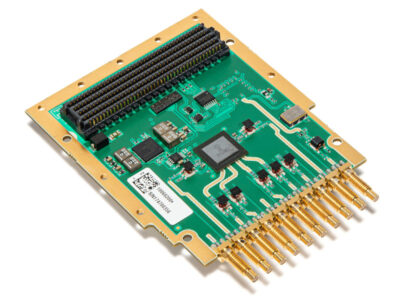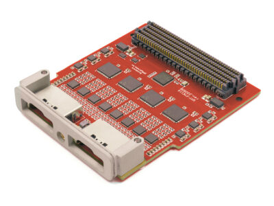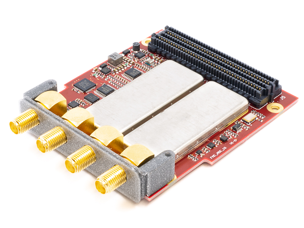
Description
The following features are controllable by software:
- Input signal range, coupling, termination and offset adjustment
- Self-calibration
- Sampling clock selection
- Direction of external trigger in/out
- ADC configuration and status
The offset adjustment does not clip the signal at the highest range (+/- 5V). That is why the “max input signal amplitude” has been specified as 10V, even though the selection of signal ranges only goes up to 5V. This way, a +10V pulse with -5V offset could still be digitised without clipping.
The sampling clock is derived from a voltage-controllable 125MHz clock source, controlled via an SPI DAC.
A copy of the 125MHz clock source is available on the FMC connector pins.
Software can select either one of the input channels to be sampled at 2 GSPS, by interleaving the 2 ADCs.
50 Ohm input is protected from overload
8 channel 12 bit I2C ADC monitors all local power supplies
This is a product that was developed in conjunction with CERN’s Open Hardware Repository and is available as a project here. The CERN Open Hardware Licence is to hardware what the free and open-source licences are to software. It defines the conditions under which a licensee will be able to use or modify the licensed material. It shares the same principles as free software or open-source software: anyone should be able to see the source – the design documentation in the case of hardware – study it, modify it and share it.