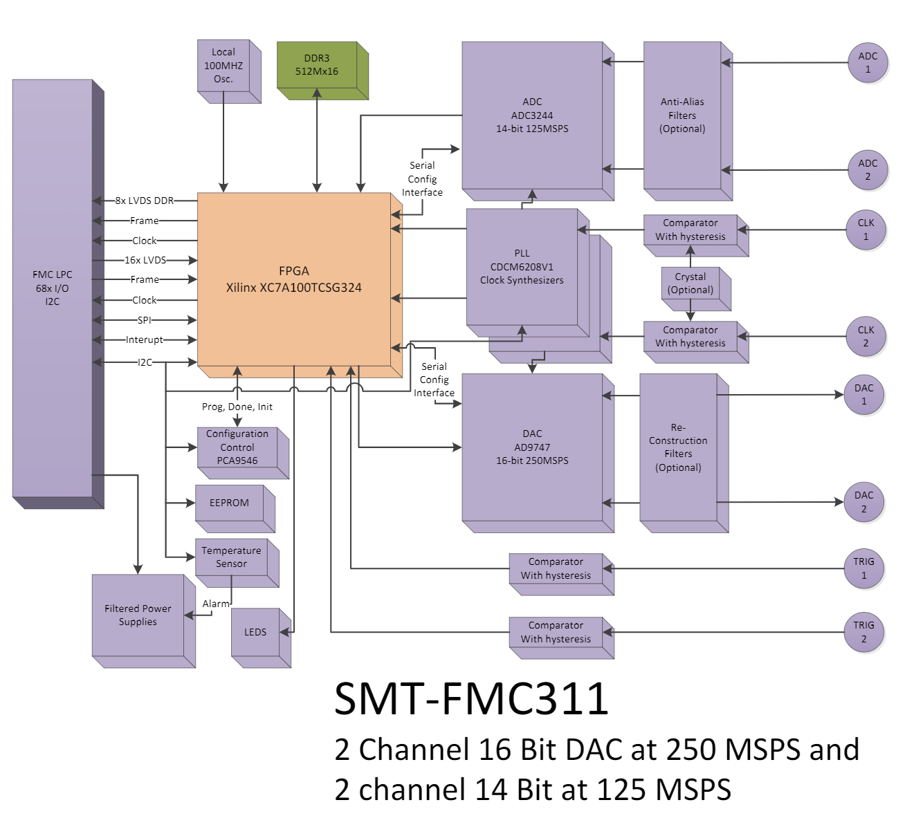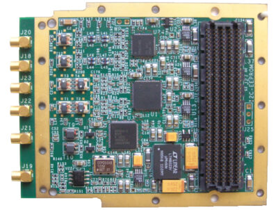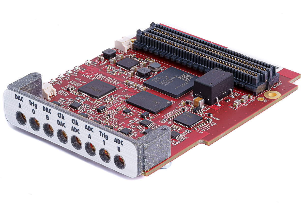


Description
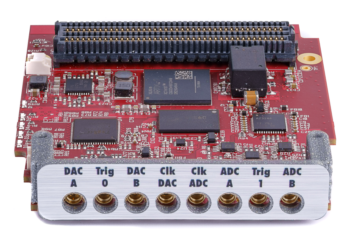
- VITA57.1 FMC-LPCTM (subset, no MGT) mezzanine.
- One dual-channel ADC.
- One dual-channel DAC.
- PLL clock synthesizer.
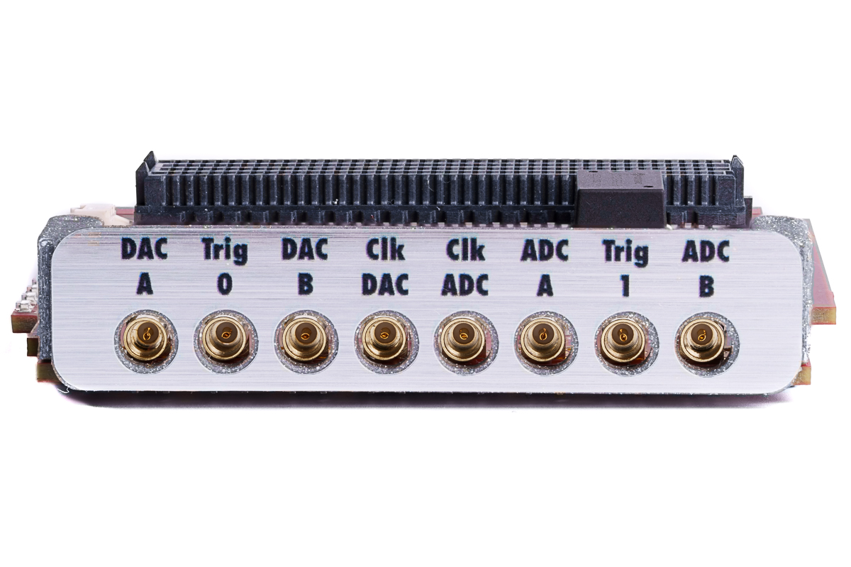
- External clock and trigger inputs.
ADC
The SMT-FMC311 includes a single TI ADC3244 device. This is a dual 14-bit ADC able to sample from 15 up to 125MSPS. It has a maximum power dissipation of 325mW (typically 233mW). SNR is typically around 72dBFS and SFDR around 90dBc.
The data interface to the FPGA is by means of two DDR LVDS pairs (per channel). This data is clocked into the FPGA by the ADC signal Bit_Clock, which is derived from the synthesiser clock to the ADC.
The ADC’s internal registers are configured over a 4-wire serial interface from the FPGA.
A total of 18FPGA I/O pins are required with a bank voltage of 1.8V. See the FPGA pin allocation below for details.
The analogue inputs are DC coupled and driven to the ADC via single-ended to differential op-amps. The input range for full scale is 2.2Vpp, with an impedance of 50Ω. Bandwidth is 50MHz (1dB). Absolute maximum input amplitude is 20dBm (min.).
Anti-alias filter options include:
- An on-board 4thorder (24dB/octave) low pass filter constructed using two op-amp stages (single device package).
- A custom surface mount module replacing the input stage components.
- An externally connected unit, e.g. Mini-Circuits (as an example) produce many suitable in-line filters with differing responses. For example, the BLP-21.4-75+ has a -3dB point at 24.5MHz and is approximately -86dB at 62.5MHz.
Analogue input connectors are either SMA or SSMC. If SMA is selected, then only the ADC and DAC connections are available on the module itself. Access to the triggers and clocks is via underside mounted MMCX connectors. A mezzanine board is available that converts from MMCX to SMA
DAC
The module includes a single Analog Devices AD9747 device. This is a dual 16-bit DAC able to operate from 0up to 250MSPS. Power dissipation is 355mW maximum (typically 310mW). SFDR is around 82dBc.
The data interface to the FPGA is by means of two 16-bit LVCMOS parallel buses (one per channel). This data is clocked into the FPGA by the DAC signal DCO (Data Clock Output), which is derived from the synthesiser clock to the DAC.
The DAC’s internal registers are configured over a 4-wire serial interface from the FPGA.
The analogue outputs are DC coupled and provide a 2.2Vpp drive (full scale) into a 50Ω load. Bandwidth is 50MHz (1dB).
Together with additional reset and control pins, a total of 38 FPGA I/O pins are required with a bank voltage of 3.3V.
Output reconstruction filter options are similar to the ADC anti-alias options.