Description
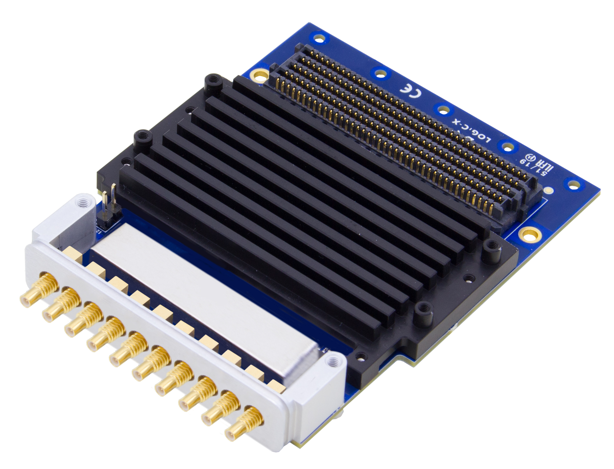
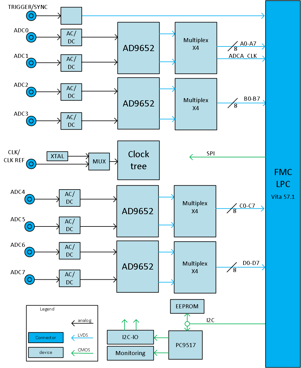
The LXD11K8 provides eight 16-bit A/D channels with up to 310 Msps data rate. All the data interfaces are based on LVCMOS and LVDS signalling. The design is based on the Analog devices AD9652 analogue to digital converters.
Analog input and output
Depending on the application requirements it is possible to order the LXD11K8 with either a DC coupled or an AC coupled analogue front end. The DC coupled interface is meant for signal acquisitions in the first Nyquist zone while the AC coupled inputs also offer the option for signal acquisition in the second Nyquist zone.
16 bit
The ADCs offer 16-bits resolution further contributing to achieving best in class signal to noise ratios.
LVDS signalling
The ADC devices make use of LVDS signaling for their data interfaces. This allows easy integration of the LXD11K8 into user FPGA designs without the need to acquire expensive and complex JESD204B interface cores. Furthermore the low pin count implementation make sure the card can be used on all Xilinx development boards as well as the Logic-X FPGA FMC carrier boards.
Clock tree
The onboard low noise clock generator ensures easy integration into small single board systems as well as standalone operation. For larger systems, it is possible to easily synchronize multiple boards by providing an external reference clock. This is a special feature offered by the onboard clock PLL.
Applications
Systems that will benefit greatly from this product are:
- MIMO Applications
- Radar waveform receivers
- Digital Beam Forming
- Medical systems
- Telecommunication systems
- Experimental Physics
- Analog playback systems
- Aerospace and test instrumentation
- Software defined radio (SDR)


