Description
Features
- 1 Independent Receivers (Rx) with FIFO
- 1 Independent Transmitter (Tx) with FIFO
- Decoding signals interface type
- 16-Bit Data-bus
- Direct addressing of all Registers
- ARINC 429 Interface: ‘1’ and ‘0’ Lines, RZ code
- Support all ARINC 429 Data Rate Transfer and up to 2.5 Mbit/s
- Multi-Label Capability
- Parity Control: Odd, Even, No Parity, Interrupt Capability
- Independent Interrupt Request Line for Rx and Tx Functions
- FPGA speed grade operating frequency dependent: system clock up to 70 MHz
- Available in VHDL source code format for ease of customisation
- DO254 design, verification and traceability documentation available on request
- Can be customised by Logic Design Solutions
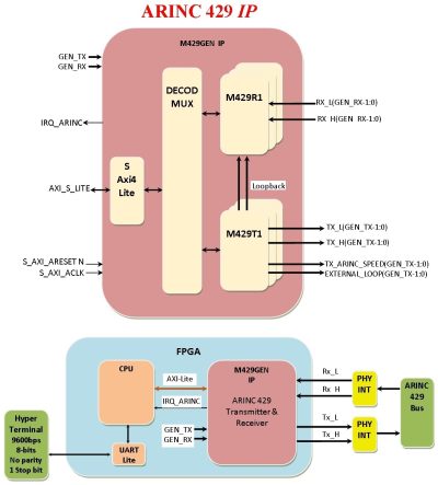
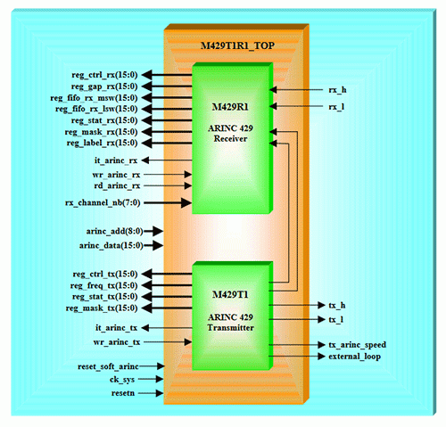
General Description
The M429T1R1 macro implements a synchronous single-chip ARINC 429 Transmit and Receive Controller Macro capable of linking one CPU to one ARINC 429 bus. The macro controls all ARINC 429 bus-specific sequences, protocol and timing. The M429T1R1 macro interface allows the parallel-bus microprocessor to communicate bidirectionally with the ARINC 429 bus. This macro can be customised according to specific needs (application-specific requirements). Any other pre-designed functions can be integrated into the FPGA. FPGA density and I/O requirements can be defined according to customer specifications.