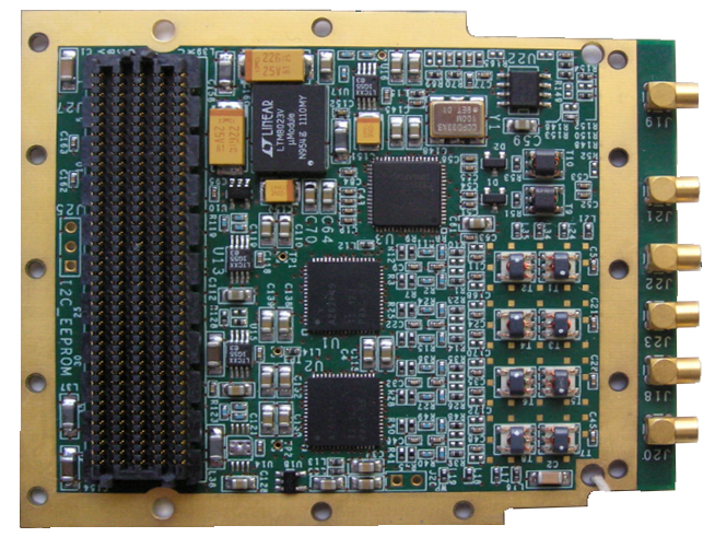
Select Page

QUAD_ADC

The QUAD_ADC is a four channel A/D FMC daughter card. The card provides four 14-bit A/D channels.


CONTACT US FOR INFO

Description

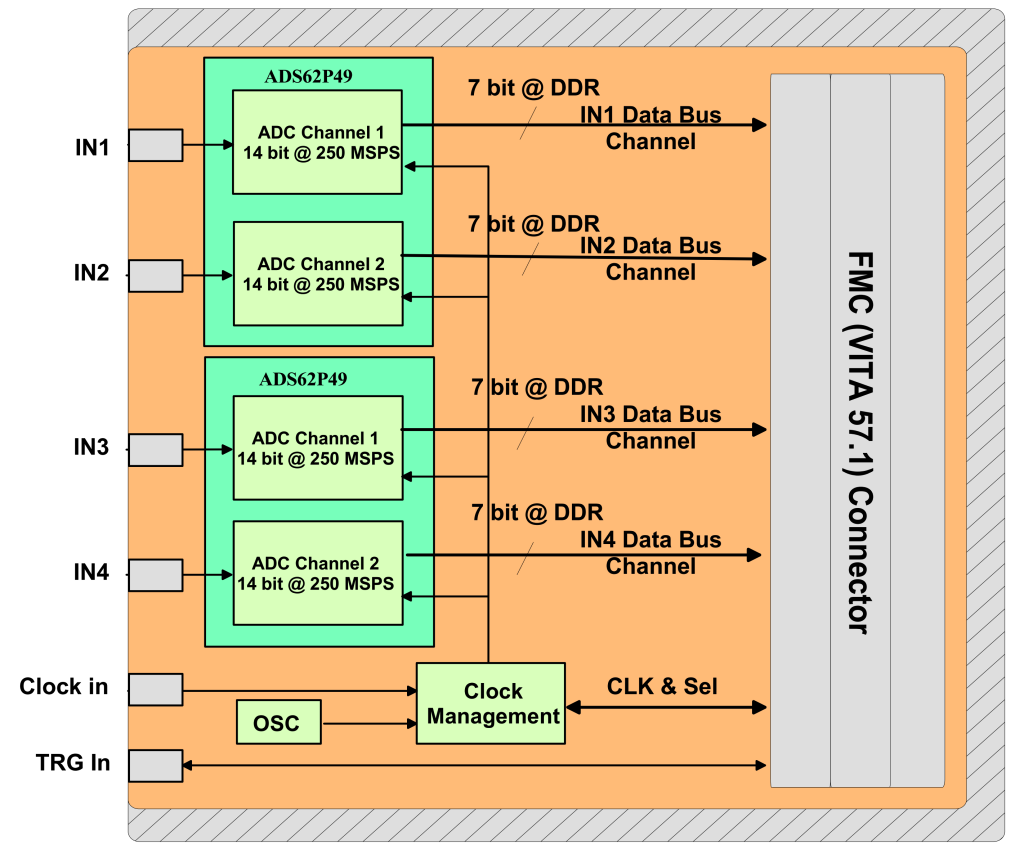
The QUAD_ADC is a four channel A/D FMC daughter card. The card provides four 14-bit A/D channels. The ADC can be clocked by an internal clock source(OCXO) or an externally supplied sample/reference clock. There is also an external trigger input for customized sampling control.

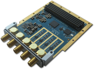
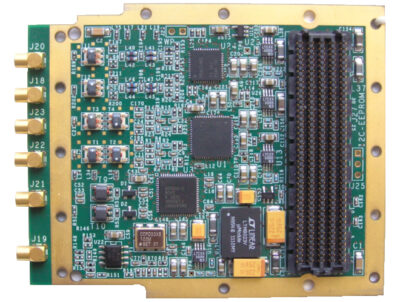
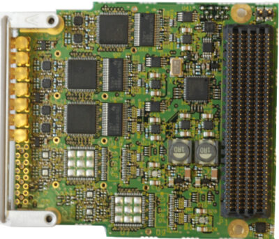
The QUAD_ADC daughter card is mechanically and electrically compliant to FMC standard (ANSI/VITA 57.1). The board has a high-pin count connector, front panel I/O, and can be used in a conduction-cooled environment. The design is based on two TI’s ADS62P49 dual channel 14-bit 250Msps ADC. The analogue signals are AC coupled, connecting to MMCX coax connectors on the front panel.

Specifications

  • Two Dual ADCs ADS6249P by T.I :
    • N. Bit 14;
    • Max clock 250 MHz;
    • Input Bandwidth selection (opz.);
    • Instantaneous Bandwidth 500 MHz;
    • Power Dissipation 1.25 W;
    • SFDR : Fin = 170 MHz 95 dBc (typ);
    • SINAD: Fin = 170 MHz 70 dBFS (typ);
  • Industrial range (-40°;+85°C);
  • Conformal Coating (opz); Anti-Sulfur Resistor type.
  • External or internal Clock Generation;
  • Input Trigger signal;
  • VITA 57.1-2010 compliant (HPC Connector);
  • LVDS/2.5V I/O Signaling;
  • Conduction Cooled;
  • Operating Temperature -40° +85°;

Applications

  • Direct RF Down Conversion.
  • Software-defined radio (SDR).
  • RADAR/SONAR.
  • Ultra Wideband Satellite Digital Receiver.
  • Aerospace and test instrumentation.

Block Diagram