Description
The most powerful Carrier Card for SOM Modules
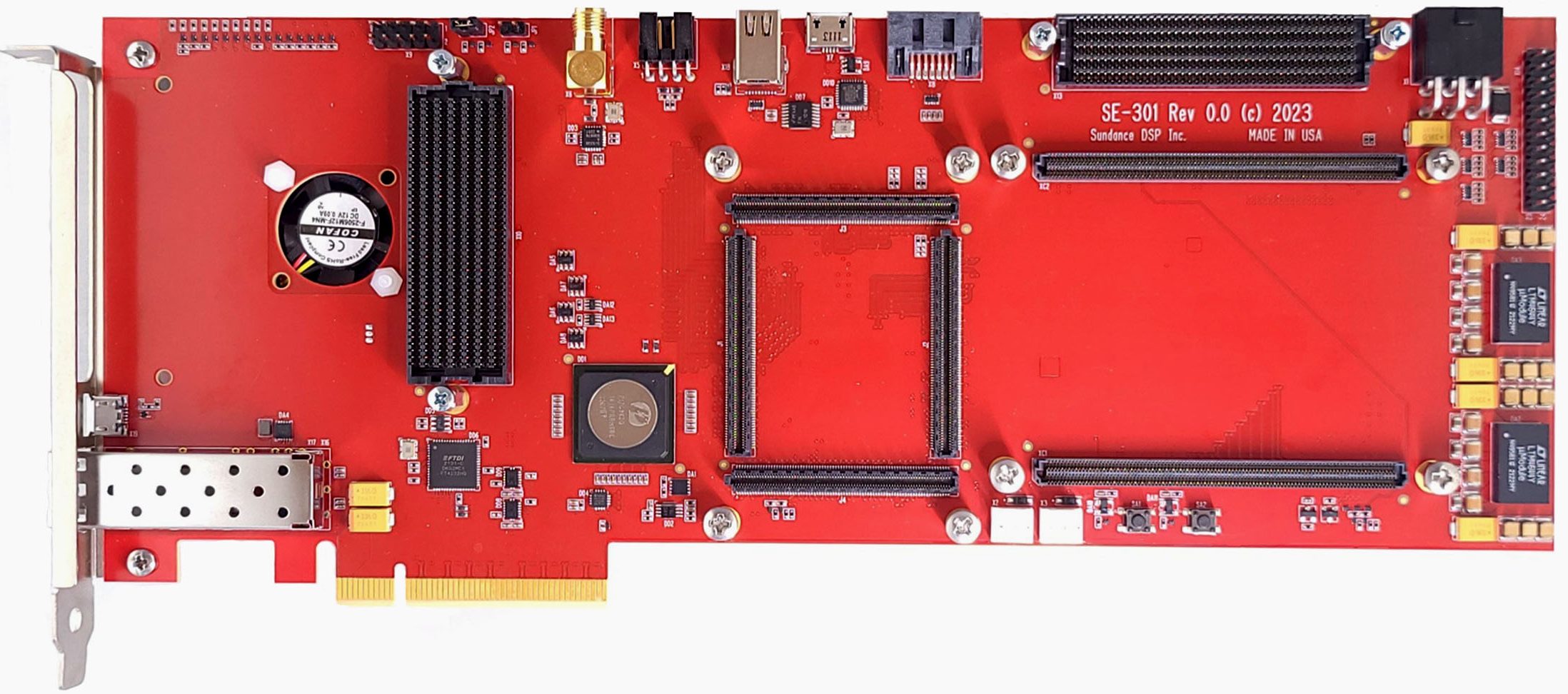
SE301 is an 8-lane PCIe card with 2 slots: one for a SoM1, based on a MPF500T, and another for a SoM1-SOC based on a MPFS460T FPGA.
SE301 is the ultimate board for Polarfire-based SoM Modules that lets you use two Polarfire SoMs simultaneously and access all of their features through one platform. The SE301 board can be used as a stand-alone device testbench or integrated into a PC using a PCIe slot. Seamless programming and debugging of the board is available by using a USB/UART-JTAG bridge via the front panel accessible micro-USB port. The FMC and FMC+ mezzanine connectors can be used to further expand the capabilities of the platform by using mezzanine cards available from SDSP or a multitude of 3rd party vendors.
The SE301 board is a perfect solution for a myriad of modern applications, such as wireline access networks and cellular infrastructure, defense and commercial aviation markets, industrial automation and IoT markets, edge computing markets, and AI/ML markets. The Polarfire SoM modules offer low-power consumption, high-performance transceivers, memory interfaces, data security features, design security features, and a multi-core RISC-V processor subsystem that are ideal for these applications.
A major advantage of Polarfire FPGAs is their instant “ON” feature which allows the device to boot immediately. Fast boot times are critical as in applications where the power to the system is disconnected, the system becomes ready instantly after power is asserted.
Features of the SE301 Board
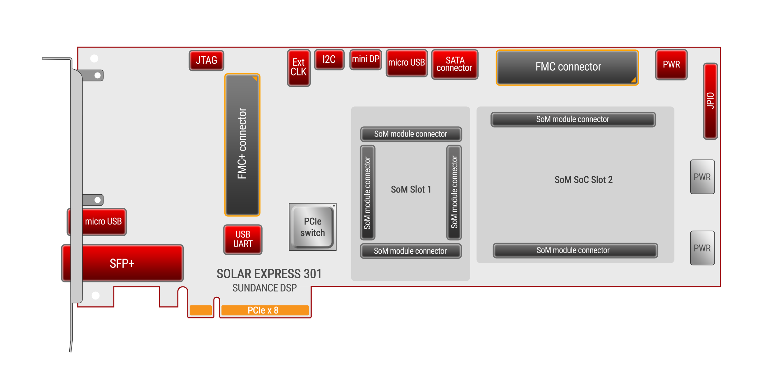
The Se301 board has two slots for SoM modules: Slot 1 and Slot 2. Slot 1 is compatible with the MPF500 Polarfire (SoM1), which is a low-power FPGA module with high-performance transceivers and DDR4 memory interfaces. Slot 2 is compatible with the MPFS460 Polarfire SoC (SoM1-SOC), which is a system-on-module with a multi-core RISC-V processor and a low-power FPGA fabric. You can also use other variants of these modules, such as the MPF300T or the MPFS250T-1152, with some limitations.
The onboard FMC+ (ASP-184329-01) connector on this board can optionally be assembled to have some GPIOs connected to slot 2. This configuration will violate the Vita 57.4 FMC+ standard but allows the mezzanine card to have the capability to be leveraged from either device simultaneously.
Seamless Development with Versatile Connectivity Options
The SE301 is an exceptional carrier card specifically designed to complement SDSP’s SOM1 and SOM1-SOC modules. This innovative board serves as a versatile platform for seamless development, offering a wide range of connectivity options to meet your project’s requirements. With its flexible design, the SE301 empowers developers to unlock the full potential of their SOM modules.
Enhanced Connectivity Options for Maximum Flexibility
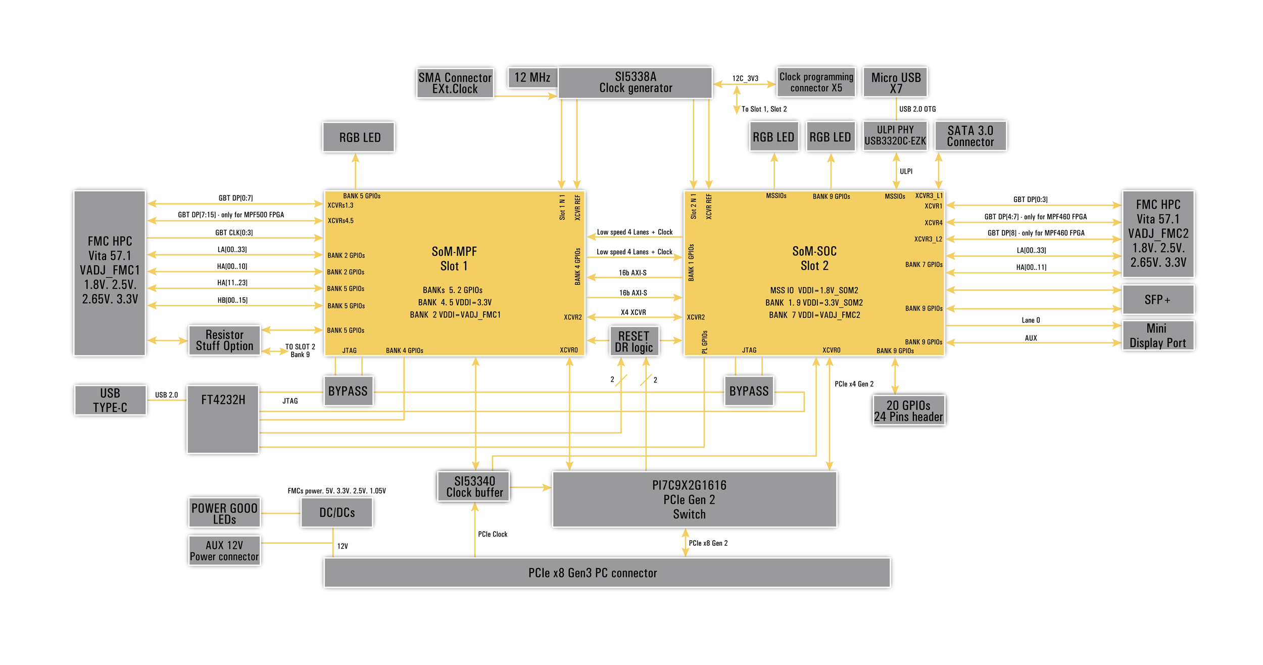
The SE301 provides a comprehensive set of connectivity options to support your development needs. With an FMC+ slot, FMC slot, SFP+ module, SATA, USB, and other peripherals available on the carrier card, you can easily integrate various external devices and expand the functionality of your SOM module-based system. This flexibility ensures compatibility with diverse application scenarios and allows for the creation of innovative solutions.
Seamless Integration and Power Options
The SE301 offers seamless integration into your development environment. It can be conveniently plugged into a PC’s PCIe slot, drawing power directly from the PCIe interface. Alternatively, it can function as a standalone board, powered through a 6 pin standard PCIe AUX power connector, providing you with the flexibility to adapt to different setups and project requirements.
Versatile Compatibility with SDSP’s SOM Modules
The SE301 is fully compatible with both the SOM1 and SOM1-SOC modules. Each module will be directly connected to PCIe if used in conjunction with a host PC. There are robust inter-module communication routes via GPIOs and transceivers too.

