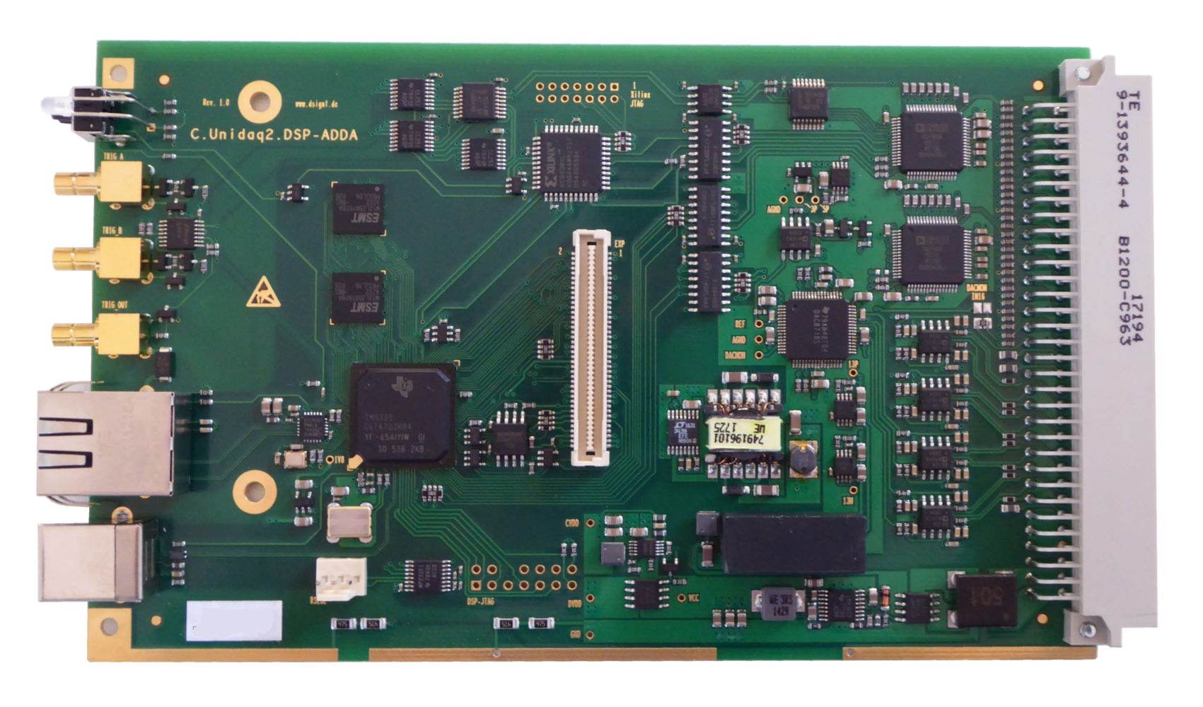
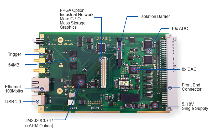
Select Page

UniDAQ2.DSP-ADDA Processor Board

£850.00


Datasheet
UniDAQ2 is a versatile data acquisition and processing system for industrial applications, scientific research and education.

16 simultaneously sampled analogue inputs with excellent performance and low latency make UniDAQ2 ideally suited for high-precision measurements of dynamic signals and control loops. Eight analogue outputs control actuators, generate stimuli signals, references or monitor internal processing states.

Category:

Description


Application Areas

  • vibration analysis and machine monitoring
  • acoustic measurements, microphone array processing
  • servo control and positioning systems
  • measuring devices for research, development, and test stands
  • laboratory equipment for education classrooms

Key Features

  • 16 simultaneously sampling SAR A/D converters, 16-bit, 175kS/s
  • 8 inherent monotonic D/A converters, 16-bit, 105kS/s
  • internal or external sampling triggers for ADC and DAC
  • 456 MHz floating-point DSP (TMS320C6747) with 64 Mbytes SDRAM
  • USB2.0 Device Port and 100Base-T Fast Ethernet
  • expansion port for mass storage, fieldbusses, display, GPIO, FPGA, etc.
  • isolation barrier between analog and digital circuits
  • single-supply power 5-18V, typ. 3W

Specifications


Input Characteristics

Number of Channels 16 single-ended (8 differential), simultaneous sampling
ADC Resolution 16 bits
Type of ADC Successive approximation register (SAR)
Sampling Rate 0 – 175 kS/s, internal or external sampling clock
Input Range ±5 V and ±10 V, programmable
Input Coupling DC
Input Impedance 1 MOhm || 10pF
Input Leakage 1.5µA typ.
Overvoltage Protection ±36 V, Input current during overvoltage conditions max ±10mA
Antialias Filter 2nd order Butterworth, -3dB cutoff 15 kHz (±5V Range), 23 kHz (±10V Range)
DNL ±0.5 LSB typ, < ±1 LSB max
INL ±0.5 LSB typ, ±2 LSB max
Zero Error < 2 mV
Full Scale Error < 0.3%
Channel to Channel Phase Mismatch <0.1° at 1kHz, <0.5° at 10kHz input frequency
Crosstalk -115dB to adjacent channel, 10kHz full-scale input signal
Latency 6 µs from sampling clock to ADC1,5,9,13 data available in DSP
10µs until all ADC channels are available in DSP
Dynamic Characteristics (input 1kHz sine, -1dB full scale, 100kS/s, no oversampling)
SINAD 87 dB
THD -100 dB
SFDR 108 dB

Output Characteristics

Number of Channels 8 single-ended, simultaneous sampling or single-DAC update mode
DAC Resolution 16 bits
Type of DAC String DAC, inherently monotonic
Sampling Rate 0 – 105 kS/s, internal or external sampling clock. Simultaneous sampling
synchronized to ADC or triggered by an independent clock source.
Settling Time full scale step: 10us to 0.03%, 15us to 1LSB
Output Range ±5 V and ±10 V, programmable
unipolar and asymmetric output range by programming the DAC offset register.
Gain and zero calibration registers per channel.
Startup Voltage 0V
Output Coupling DC
Output Impedance 50 Ohms
Current Drive ±5mA, short-circuit limited to 70mA
Capacitive Drive 20000pF
Antialias Filter 2nd order Butterworth, -3dB at 50kHz
DNL ±0.5 LSB typ, ±1 LSB max
INL ±1.5 LSB typ, ±4 LSB max
Zero Error < 3 mV uncalibrated
Full Scale Error < 0.3% uncalibrated
Crosstalk -105dB to adjacent channel, 10kHz full-scale output signal
Dynamic Characteristics (output 1kHz sine, -1dB full scale, 100kS/s)
SINAD 74 dB
THD -74 dB
SFDR 75 dB

Trigger Inputs

Number of Channels 2
Input Range 3.3V and 5V TTL/CMOS compatible, Overvoltage Protection: ±36 V,
Input current during overvoltage conditions max ±10mA
Usage ADC conversion start
DAC update
Pre- or post trigger event to DSP and/or Expansion Board
Capture inputs (frequency, pulse width, duty cycle)
Quadrature input (relative rotation angle and speed)

Trigger Outputs

Number of Channels 1
Output Range 3.3V LVTTL, 5V TTL/CMOS compatible
Output Impedance 50 Ohms
Usage ADC sampling clock output
Trigger event or clock output from DSP and/or Expansion Board

Communication Ports

Ethernet 1 Port, 100 MBit/s, full-duplex, RJ45
USB2.0 1 Port, 480 MBit/s, Typ B (device)

Signal Processing

DSP Texas Instruments TMS320C6747, 456 MHz, optional: OMAP-L137 DSP + ARM9
Memory 32 Kbytes L1 Program RAM/Cache
32 Kbytes L1 Data RAM/Cache
256 Kbytes L2 RAM/Cache
128 Kbytes L3 RAM
64 Mbytes SDRAM, 133 MHz
8 Mbytes non-volatile Flash Memory

Debugging Ports

JTAG TI in-circuit emulator, 14-pin header, 2.54mm pitch
Debug UART 1 x RS232, TxD and RxD, 3pin KK-connector 2.54mm pitch

Expansion Port

Connector 80-pin, 0.8mm pitch
Signals DSP EMIFA * (asynchronous parallel bus and NAND-Flash support)
DSP UHPI * (parallel host processor interface)
DSP SD/MMC * (eMMC or SD-Card expansion)
DSP LCDC * (LCD Controller)
* These signals share the same pins. With the exception of the LCD + SD/MMC
combination, usage is mutually exclusive.
4 x GPIO, unused signals of the above interfaces can be used as additional GPIO
1 x SPI
1 x I2C
Trigger Signals (2 x in, 3 x out)
Power Supply 3.3V and VIN (5 to 18V)

Power Supply

Supply Voltage 5 – 18V ±5%, reverse-polarity protected
Power Consumption 3W typical

Isolation

max. Voltage 350VAC / 500VDC between analog GND and digital GND / power supply

Mechanics

Size Eurocard, 160 x 100 x 15 mm

Operating Conditions

Ambient Temperature 0-70°C
Humidity max. 95% rel., non condensing

Application Notes


Power Grid Monitoring


PRU (Programmable Realtime Unit) Usage